


PCB Editing
This discussion is connected to the gimp-user-list.gnome.org mailing list which is provided by the GIMP developers and not related to gimpusers.com.
This is a read-only list on gimpusers.com so this discussion thread is read-only, too.
| PCB Editing | Sorceress99 | 17 Jan 08:32 |
| PCB Editing | Ofnuts | 17 Jan 09:46 |
| PCB Editing | rich404 | 17 Jan 13:19 |
| PCB Editing | Sorceress99 | 17 Jan 16:41 |

- postings
- 6
PCB Editing
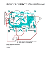
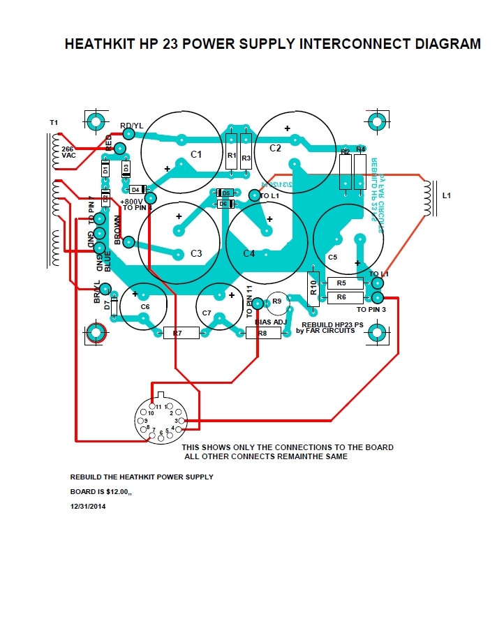
I am trying to separate the 2 sides of a printed circuit board photo and can't remember how to do it. The circuit diagram is in blue and the parts layout is in black. Wiring placement is in red is irrevelant and can be deleted. The PCB pattern, in blue, is printed on glossy photo paper on a laser printer, in black. The print is set on 'high quality' so needs to be sharp and clear. The image is then positioned, face down on a blank copper clad PCB then transfered to the board by various means such as heat lamination or chemically. Once completed, the parts layout is printed on the laser as before, positioned in alignment with the circuit side, then transfer to the opposite side of the board as before. Any help with separating the 2 images would be appreciated.
Attachments: * https://www.gimpusers.com/system/attachments/1338/original/HP-23_PCBFull.jpg
Sorceress99 (via www.gimpusers.com/forums)
-
 HP-23 PCB Upgrade
HP-23_PCBFull.jpg (196 KB)
PCB Editing
On 1/17/20 9:32 AM, Sorceress99 wrote:
I am trying to separate the 2 sides of a printed circuit board photo and can't remember how to do it. The circuit diagram is in blue and the parts layout is in black. Wiring placement is in red is irrevelant and can be deleted. The PCB pattern, in blue, is printed on glossy photo paper on a laser printer, in black. The print is set on 'high quality' so needs to be sharp and clear. The image is then positioned, face down on a blank copper clad PCB then transfered to the board by various means such as heat lamination or chemically. Once completed, the parts layout is printed on the laser as before, positioned in alignment with the circuit side, then transfer to the opposite side of the board as before. Any help with separating the 2 images would be appreciated.
Attachments: * https://www.gimpusers.com/system/attachments/1338/original/HP-23_PCBFull.jpg
In the monochrome channel mixer
* pushing red to 100% makes the red channel disappear
* You can substract a bit of green from blue or vice-versa to make the printted circuit grey
Duplicate the resulting layer
Color>Invert on the top layer
Put the top layer in "difference" mode: the grey bits are about the same in both image, so they becomes 0 (black) while the black and white parts are changed to their opposite and the difference ins close to 255 (white).
Still some cleaning left to do, and painting where the red tracks have left white lines in the circuits.
Personally for such a small circuit, I would redraw it, you need a couple of brushes for the solder points, a brush to draw straight lines, and wider areas can be filled with the polygon selection.
PCB Editing
I am trying to separate the 2 sides of a printed circuit board photo and can't
remember how to do it. The circuit diagram is in blue and the parts layout is
in black. Wiring placement is in red is irrevelant and can be deleted. The PCB
pattern, in blue, is printed on glossy photo paper on a laser printer, in black.
The print is set on 'high quality' so needs to be sharp and clear. The image is
then positioned, face down on a blank copper clad PCB then transfered to the
board by various means such as heat lamination or chemically. Once completed,
the parts layout is printed on the laser as before, positioned in alignment with
the circuit side, then transfer to the opposite side of the board as before. Any
help with separating the 2 images would be appreciated.Attachments: *
https://www.gimpusers.com/system/attachments/1338/original/HP-23_PCBFull.jpg
That image is on the small side + jpeg arifacts Does not make for wonderful quality.
You can get most of your requirement using the gmic gimp plugin from www.gmic.eu
I would do it as this 3 minute video: https://youtu.be/9esPa-CP628
but plenty of repair still required.
rich404 (via www.gimpusers.com/forums)
- postings
- 6
PCB Editing
That image is on the small side + jpeg arifacts Does not make for wonderful
quality.You can get most of your requirement using the gmic gimp plugin from www.gmic.eu
I would do it as this 3 minute video: https://youtu.be/9esPa-CP628
but plenty of repair still required.
Thanks Rich. I will get the gmic plugin but I think I the last time I did something simuliar was to 'pick' each color and just delete them. Delete the red and black colors and leave the blue. But I don't see how I did it that way with the commands I have. I will try the process you show in the video.
Sorceress99 (via www.gimpusers.com/forums)


